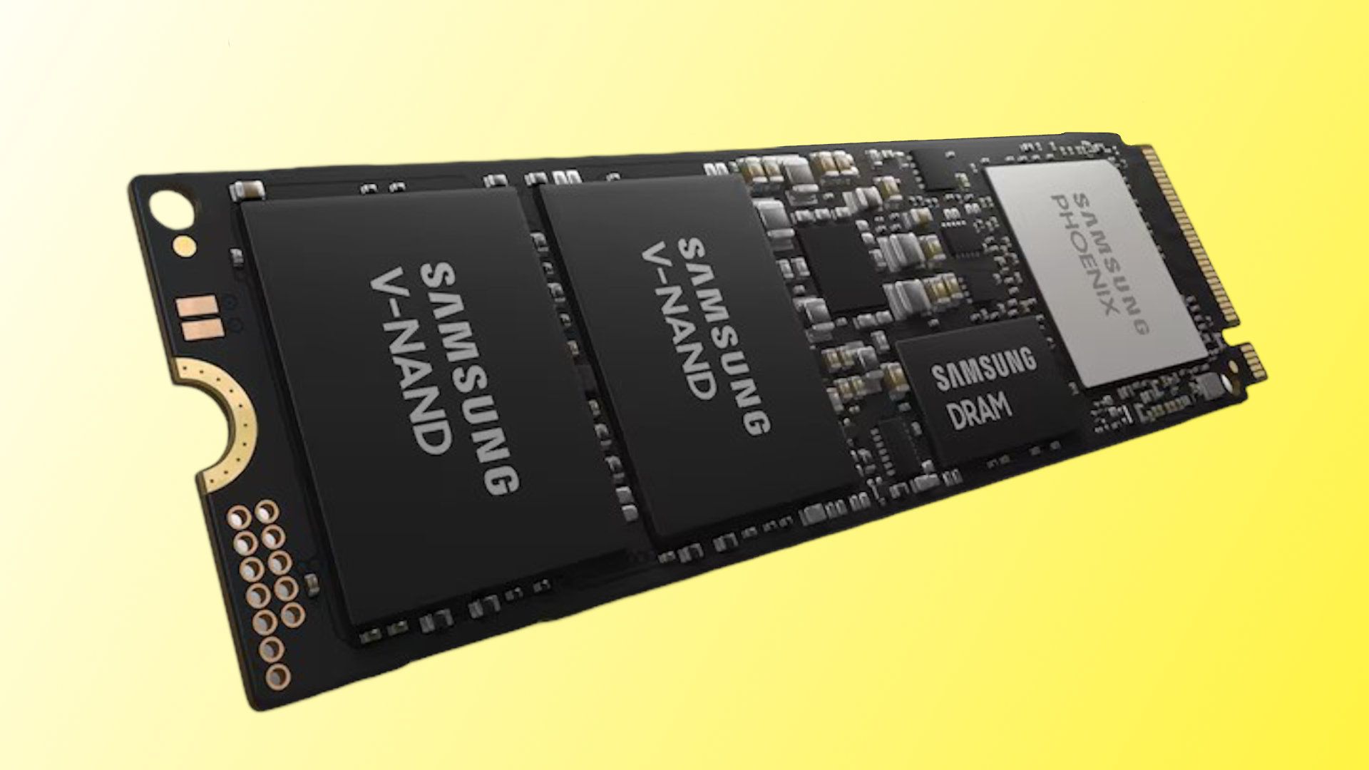
Samsung has reportedly developed 900-layer flash memory chips and I’m thinking SSDs could get seriously cheap if this AI bubble ever pops
Samsung has reportedly developed a prototype NAND flash memory chip with an unprecedented 900 layers, created by bonding two 450-layer cell wafers together using Cell Multi-Bonding (CMB) technology. This advancement significantly surpasses the current industry record held by SK Hynix, whose highest-density NAND memory currently tops out at 321 layers. The South Korean electronics giant is also preparing its own 10th Generation V-NAND technology with over 400 layers for market release.
This development represents a major step forward in memory density and storage capacity. Higher layer counts in NAND flash memory enable manufacturers to store more data in the same physical footprint, potentially reducing production costs and leading to more affordable storage solutions across consumer devices. As the density of memory chips increases, the cost per gigabyte of storage theoretically decreases, which could translate to cheaper SSDs for consumers.
The timing of this breakthrough coincides with ongoing speculation about market dynamics in the tech industry. While Samsung’s focus remains on pushing the boundaries of memory technology, industry observers have noted that significant advances in storage capacity could eventually impact pricing in the SSD market if demand shifts or market conditions change.